

We have found that our members are often taking on graduates and then putting them through bespoke training once or twice a year, which can take up valuable internal resource.
This can be happening many times at individual companies – here at DESN we are looking to support industry by creating these training programs and running them on behalf of industry – specifically focussing on some of the key knowledge gaps identified from within our working groups.
These courses are run on behalf of industry and managed by industry, our members have direct input into the modules and course direction to ensure its valid and relevant to them, with the flexibility to be able to make changes as industry demands change.
By working with members both large and small , everyone benefits from the same training and costs are applied equally, so smaller companies are able to access specific content that may have previously been out of reach.
DESN is not a training provider, but works with third party companies and our own members to provide content, by providing multiple students to our providers, DESN members are able to achieve course discounts which can produce significant savings during the year.


Currently Available Courses

Introduction to Design Verification
Course Objectives
By the end of the course, participants should be able to:
- Describe the best-practice DV strategies applied currently to semiconductor digital designs
- Understand the main methodologies, tools and languages used in those best-practice DV strategies
- Apply those DV methodologies, tools and languages to basic digital designs
- Analyse a “real” semiconductor digital design and suggest an appropriate DV strategy
- Understand current best-practice DV sufficiently to enable participants to discuss DV topics confidently with colleagues
After completing the course participants will have sufficient understanding of DV tools and methodologies to contribute effectively to real projects
2 Target audience
1. University students going on or started a placement at a semiconductor design company
2. University graduates starting or started work at a semiconductor design company
3. Engineers wanting to transition their career to or are just curious about DV
4. Managers wanting some understanding of the topic
3 Pre-requisites
None. The course is suitable for a wide range of people working in semiconductor design & development, especially recent graduates. Although not a perquisite, some experience of programming (preferably with an Object-Oriented language) would be useful.
4 Course overview and structure
The course runs over 1 month with the following main activities:
1. 8 online one-hour lectures covering the major DV topics (details)
a. Supported by exercises (using both SystemVerilog and VHDL) (details)
2. 4 online one-hour lectures covering debug (details)
a. Supported by exercises (using both SystemVerilog and VHDL) (details)
3. Access to tools in the cloud for running online exercises (details)
a. There will also be a non-cloud option that allows participants to download the exercises and run them on there own machine with their own licenses.
4. Access to online Cadence courses using the latest languages, tools and techniques (limited access) (details)
More details on the above are given in the 3 sections below.
Note that participants will get additional support outside the lectures and exercises as needed.
Preparatory and follow-on reading will be suggested but neither are obligatory. There is no (summative or formative) assessment (details).
5 DV lectures: Details
The online DV lectures will cover the following
1. Introduction What is Design Verification?
Verification complexities
The cost of bugs
2. Simulation-based Verification Driving stimulus and Checking responses
Observability and Controllability
Black box vs. white box
Verification hierarchy
Verification tools
3. Hardware design and verification languages Levels of abstraction
Overview of Verilog
Overview of System Verilog
4. The Verification Cycle Verification planning
Verification Methodologies
Planning, milestones, tracking and completion criteria
Functional coverage and coverage closure
5. Stimuli generation
Checking Foundations
Online vs. offline, static vs. dynamic
Constrained random automation
What and when to check
Checking mechanisms
6. Coverage Introduction
Code coverage
Functional coverage
Coverage analysis and closure
7. Assertion Based Verification Benefits and drawbacks of assertions
Types of assertions
Assertion libraries
Writing assertions and properties
8. Verification in practise The verification cycle from start to finish
IP level verification in practise
SoC level verification in practise
6 Debug lectures: Details
The online DV lectures will cover the following
1. Introduction to debug What is debug and where do bugs lie?
Debugging designs and verification environments
Working with (not against the design team
2. Making debug efficient Techniques to reduce debug time
3. Making debug effective Ensuring a bug is fixed
Making use of “bug clustering”
4. Design verification environments for debug How can I ensure my verification environment is design for ease of debug?
7 Exercises: Access to exercises and DV tools
Participants will be given access to some small DV exercises (take exercises to mean both examples and exercises) to support what is being taught in both the DV and the debug lectures. The exercises will be available in both SystemVerilog (some using UVM) and VHDL (some using OSVVM):
• Small design and test bench exercises will be provided to allow participants to implement the concepts they have learned in the lectures
• There will be support for using the tools, running the exercises and implementing the suggested updates.
• The exercises and changes will be kept small and simple due to time limitations
o They will start with directed test exercises (adder, FIFO, etc)
o There will be separate exercises for assertions
o There will also be small UVM/OSVVM exercises to allow students to see how a complete constrained random UVM/OSVVM test bench can be constructed
o For all exercises, students will ONLY be asked to complete a small exercises rather than construct a new test bench from scratch
o There will be full solutions available for every exercise
The exercises will be available on 2 platforms: the cloud; and download.
7.1 Online in the cloud
Online tools for running and updating the exercises.
• All participants will be given access to an Amazon cloud server dedicated for use with the course
• Participants will get access to tools to allow them to run simulations, perform debug, edit test benches and measure coverage (code and functional)
o Students will be allowed to download their solutions but uploading by students will be prohibited
7.2 Download
Students will be able to download the exercises for running on their own machines with their own tools and licenses.
8 Limited access to Cadence self-paced online course content
Students will have free access to Cadence courses through their university for self-study. Some corporate participants may also have access through their Cadence corporate access.
There are 4 suggested Cadence courses with the first of these being recommended and supported on this course:
• SystemVerilog Accelerated Verification with UVM (details)
• Verilog Language and Application (details)
• SystemVerilog for Design and Verification (details)
• JasperGold Formal Fundamentals (details)
8.1 SystemVerilog Accelerated Verification with UVM
Duration is 32 hours online. Content from Cadence website:
• Introduction to UVM Methodology and Universal Verification Component (UVC) Structure
• Overview of the Router Lab Project
• Stimulus Modeling
o Declaring data items
o Field automatio and data operations (copy, clone, print, etc.)
• Simulation Phases
o Standard and run-time phasing
• Test and Testbench Classes
o Testbench layer
o Test and test selection
o Reports
• Creating a Simple Environment
o UVM component classes
o Structure of a simple environment
o Packaging and directory structures
• Configuration
o Configuration database (uvm_config_db)
o How configuration works, with rules, examples and debugging
o set_config method calls (deprecated in UVM1.2)
• Type Overrides and the Factory
o Constraint layering and behavior modification
o Factories
o Type and instance overrides
• UVM Sequences
o Sequence structure
o uvm_do macros
o Alternatives to uvm_do macros
o Nested sequences and sequence properties
o Sequence selection
o Objection mechanism for stopping simulation
o Objection changes in UVM1.2
• Connecting to a DUT
o Virtual SystemVerilog interfaces
o Assigning interfaces using the configuration database
• Interface and Module UVCs
o Integrating multiple UVCs
o UVCs with multiple agents
o Configuration objects
• Multichannel Sequences (virtual sequences)
o Virtual sequencers
o Defining virtual sequences
• Building a Scoreboard
o Scoreboard requirements and considerations
o Connecting components with TLM analysis interfaces
o Hierarchical connections with export
• Transaction-Level Modeling (TLM)
o Concepts and terminology
o Simple, unidirectional connections (put, get, peek)
o TLM FIFO
o Scoreboards with TLM analysis FIFO
o TLM2
• Functional Coverage Modeling (Optional)
o Coverage-driven verification overview
o Coverage considerations in a UVC
• Introduction to Register Modeling
o Overview of the purpose and structure of register modeling
o Generation of a register model
o Integration into an environment
o Simulation using built-in and user-defined register sequences
• Conclusions
8.2 Verilog Language and Application
Duration is 32 hours online. Content from Cadence website:
• Describing Verilog Applications
• Language Introduction
• Choosing Between Verilog Data types
• Using Verilog Operators
• Making Procedural Statements
• Using Blocking and Non-Blocking Assignments
• Using Continuous and Procedural Statements
• Understanding the Simulation Cycle
• Using Functions and Tasks
• Directing the Compiler
• Introducing the Process of Synthesis
• Coding RTL for Synthesis
• Designing Finite State Machines
• Avoiding Simulation Mismatches
• Managing RTL Coding Process
• Managing the Logic Synthesis Process
• Coding and Synthesizing an Example Verilog Design
• Using Verification Constructs
• Coding Design Behavioral Algorithmically
• Using System Tasks and System Functions
• Generating a Test Stimulus
• Developing a Testbench
• Example Verilog Testbench
8.3 SystemVerilog for Design and Verification
Duration is 32 hours online. Content from Cadence website:
• SystemVerilog Overview
• Standard Data Types and Literals
• Procedures Statements and Procedural Blocks
• Operators
• User-Defined Data Types and Structures
• Hierarchy and Connectivity
• Static Arrays
• Tasks and Functions
• Interfaces
• Simple Verification Features
• Clocking Blocks
• Random Stimulus
• Basic Classes
• Polymorphism and Virtuality
• Class-Based Random Stimulus
• Interfaces in Verification
• Covergroup Coverage
• Queues and Dynamic and Associative Arrays (QDA)
• Introduction to Assertion-Based Verification (ABV)
• Introduction to SystemVerilog Assertions (SVA)
• Direct Programming Interface (DPI)
• Interprocess Synchronization
8.4 JasperGold Formal Fundamentals
Content from Cadence website
• Formal Friendly SVA Coding
o Identify SVA which is likely to be inefficient
o Create Auxiliary Code (HDL helper code) to assist when writing properties
o Recognize problems that cannot be solved by SVA alone
o Replace inefficient SVA code with a combination of simple properties and simple auxiliary code
• Introduction to Formal Analysis
o Contrast Formal with Dynamic
o Describe Formal Analysis terminology
o Describe how Formal tools work
o Explain factors affecting the quality of results
o Describe the limitations of Formal Analysis tools
o Recognize initialization issues
o Understand different kinds of formal use models and goal
• JasperGold Expert System (JGES)
o Knowledge-Based System
o Client-Based System
o Viewing and using recommendations
• JasperGold Apps Usage: Applying DLFA Flow
o Identify Focus Areas for Formal Analysis
o Design Level Formal Analysis (DLFA) flow phases, setup, initialisation, stopats, etc.
o Using ProofGrid to distribute jobs to server farms
o Intro to ProofMaster in JasperGold
o Debug Hand-off
o Constraint management and debugging
o Recommendations
o Where to get help
• Visualize
o What is Visualize?
o Visualize Flow
o Visualize GUI
o Visualize Features
• Overview of Formal Analysis Use Models
o Explain how Formal Verification differs from Simulation
o Use Formal Analysis for design exploration
o Use Formal Analysis to prove user defined functional properties
o Use Formal Analysis to perform Deep Bug Hunting (DBH)
o Apply each of the different JasperGold Apps to obtain verification closure
• Causes of Complexity
o Understand contributing factors to formal complexity
o Understand what adds state to the proof and how to reduce state
o Use the JasperGold tool features to understand formal complexity
• Generic Complexity Reduction Methods
o How to simplify an environment
o Functional, value and bitwise splitting of properties to improve performance
o Structural changes
o Black-boxing
o Complexity Tool aids – Complexity Manager and Formal Profiler
• Abstractions
o Differentiate between what is an abstraction and what is a reduction
o Use abstraction mechanisms to greatly reduce the time taken for a formal proof
o Apply IVA’s to choose arbitrary configurations
o Apply Reset Value Abstractions (RVAs)
o Apply Counter Abstractions
• XPROP App
o Use the XPROP App to detect, debug and fix X-propagation issues for a variety of X-sources and destinations
o Use the –precond option to prevent real X-prop problems being masked by the waiving of false negatives
• The Verification Completeness Problem
• Review verification methodologies
• Examine case study highlighting the verification completeness problem
• State techniques for minimizing risk of verification holes
• States the merits of each verification technique
• Property Development Introduction
o Overcoming the “blank page syndrome”
o Who Writes Properties and When?
o Guidelines for Writing Properties
o Categories of Properties
o Property Development Process
o Need for Both Checks and Coverage
• Interface Property Development
o Develop black-box protocol properties
o Enumerate a finite set of fundamental behaviors for features extracted from a verification plan
o Enumerate a finite set of protocol categories with which common protocols are associated
o Identify the subset of fundamental behaviors exhibited by a given protocol category
o Use these fundamental behaviors to drive the development of the protocol properties
o General vs. specific properties and why specific properties may be undesirable
9 Assessment
The course be attendance only with no assessment. Participants who attend the course will receive the following
• For completing parts 1 and 2: students will receive a Continuing Professional Development and a TechWorks Academy certificate
• For completing part 3: A Cadence certificate of accomplishment and also a digital badge of accomplishment, which the students can include in their LinkedIn profile

Electronics Assembly for Engineers
Introduction to PCB Design for Manufacturability (Micromodules)
This series of ten micro-modules introduce some of the key concepts required to optimize the design of printed circuit boards for manufacture. If you’d like to learn more after completing the series, consider consider taking the IPC Design for Manufacturability course.
Introduction to PCB Design I
Taught by an IPC-certified industry expert with more than 25 years of experience in the field, this 6-week online program introduces participants to the concepts and skills required to create realworld designs that comply with IPC standards. This introductory course will focus on front-end design concepts such as schematic capture, library parts creation, basic electrical engineering concepts, and documentation.
Introduction to PCB Design II
In this course, participants employ the lessons learned in Introduction to PCB Design I to effectively implement their designs using techniques such as multi-layer routing, signal integrity, transmission lines, and more. The course also focuses on how manufacturing and assembly techniques impact design, documentation and manufacturing file generation.

PCB Layout
Introduction to PCB Design for Manufacturability (Micromodules)
This series of ten micro-modules introduce some of the key concepts required to optimize the design of printed circuit boards for manufacture. If you’d like to learn more after completing the series, consider consider taking the IPC Design for Manufacturability course.
Introduction to PCB Design I
Taught by an IPC-certified industry expert with more than 25 years of experience in the field, this 6-week online program introduces participants to the concepts and skills required to create realworld designs that comply with IPC standards. This introductory course will focus on front-end design concepts such as schematic capture, library parts creation, basic electrical engineering concepts, and documentation.
Introduction to PCB Design II
In this course, participants employ the lessons learned in Introduction to PCB Design I to effectively implement their designs using techniques such as multi-layer routing, signal integrity, transmission lines, and more. The course also focuses on how manufacturing and assembly techniques impact design, documentation and manufacturing file generation.
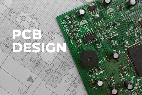
PCB Design
Introduction to PCB Design for Manufacturability (Micromodules)
This series of ten micro-modules introduce some of the key concepts required to optimize the design of printed circuit boards for manufacture. If you’d like to learn more after completing the series, consider consider taking the IPC Design for Manufacturability course.
Introduction to PCB Design I
Taught by an IPC-certified industry expert with more than 25 years of experience in the field, this 6-week online program introduces participants to the concepts and skills required to create realworld designs that comply with IPC standards. This introductory course will focus on front-end design concepts such as schematic capture, library parts creation, basic electrical engineering concepts, and documentation.
Introduction to PCB Design II
In this course, participants employ the lessons learned in Introduction to PCB Design I to effectively implement their designs using techniques such as multi-layer routing, signal integrity, transmission lines, and more. The course also focuses on how manufacturing and assembly techniques impact design, documentation and manufacturing file generation.