
Trends in Semiconductor System Design
February 6 @ 8:30 am - 5:00 pm
Trends in Semiconductor System Design

Thank you to our Sponsors

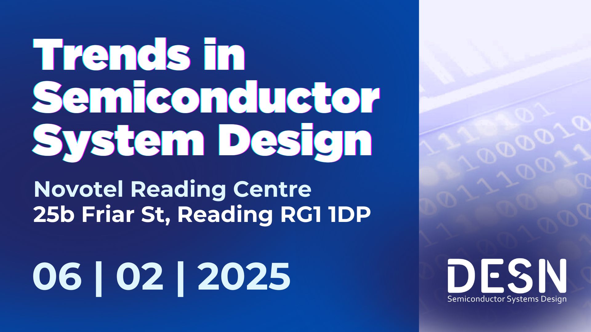
The Trends in System Design event, hosted by DESN in Reading on February 6th, will be open to both members and non-members. We will examine emerging trends in semiconductor system design, with a particular focus on how AI/ML is being used in product design and the design flow.
The event will also address the challenges in designing IP to meet the compute intensive demands of AI, including bandwidth and latency issues related to data access, SoC design challenges, and obstacles related to the latest technology nodes.
Additional topics will cover manufacturing, testing, yield challenges, and the transition to chiplets.
Participants will also discuss the process of validating and signing off chips for production, as well as cost and return-on-investment considerations.
A second major focus will be on how to best leverage AI’s potential in design flows. Key discussions will explore where AI can be deployed for maximum benefit without introducing risks such as “hallucinations” or security vulnerabilities.
Presentations will include insights from EDA companies on the features they are incorporating into their tools, as well as contributions from users who are developing their own solutions.
| Time | Event |
|---|---|
| 09:00 | Registration, arrival and refreshments |
| 09:25 | Introduction |
| 09:30 | Keynote: Chiplet Standards: A New Route to Arm-based Custom Silicon – Rob Dimond, System Architect and Fellow, Arm |
| 10:00 | The Turkey Voting For Christmas – AI and the Verification Engineer – Andrew Bond, Director – Silicon Verification, Axelera AI |
| 10:30 | Imec research: driving advancements in semiconductor technology – Bruno Jansen, Regional Managing Director, imec Cambridge UK |
| 11:00 | From Chips to Systems: Redefining Semiconductor Packaging and Integration – Dr. Jayakrishnan Chandrappan, CSA Catapult |
| 11:30 | Break |
| 12:00 | Using Generative AI to Transform Chip to Data Center Design Flows – Rod Metcalfe, Senior Product Management Group Director, Cadence |
| 12:30 | AI-Enabling a Revolution in Chip Design Productivity – Loay Qteet, Staff Application Engineer, Synopsys |
| 13:00 | Unlocking the AI Advantage with Siemens EDA Products – Sathishkumar Balasubramanian, Siemens |
| 13:30 | TechWorks AI Group – Dr Mike Bartley, Senior VP, Tessolve |
| 13:45 | Lunch followed by Close |
Speakers

Sathishkumar Balasubramanian, Senior Director of Product Management, Marketing & Biz Dev, Siemens
Unlocking the AI Advantage with Siemens EDA Products
What’s behind the excitement in the industry around AI? AI is impacting virtually every aspect of semiconductor design. Verifiably accurate AI solutions that “just work” deliver results that users can trust and accelerate schedules, while reducing the overall resources needed for chip design and verification. At Siemens EDA, we have successfully leveraged AI technologies to accelerate design and verification. In this session, we will provide an overview of state-of-the-art AI-powered solutions encompassing the entire Siemens EDA product portfolio.

Andrew Bond, Director – Silicon Verification, Axelera AI
The Turkey Voting For Christmas – AI and the Verification Engineer
As EDA embraces the new opportunities AI brings how will it change what we think of as verification.
From tooling to coding, from developing to debugging, from team dynamics to hiring how might things be about to change, and how can we be best prepared.

Rob Dimond, System Architect and Fellow, Arm
Chiplet Standards: A New Route to Arm-based Custom Silicon
A key challenge our partners are consistently looking to solve is: How can we continue to push performance boundaries, with maximum efficiency, while managing costs associated with manufacturing and yield? Today, as the ever more complex AI-accelerated computing landscape evolves, a key solution emerging is chiplets.
Chiplets are designed to be combined to create larger and more complex systems that can be packaged and sold as a single solution, made of a number of smaller dice instead of one single larger monolithic die. This creates interesting new design possibilities, with one of the most exciting being a potential route to custom silicon for manufacturers who historically chose off-the-shelf solutions.
This talk will describe the standards framework that Arm is building with our partners, and the broader industry. Including our own specifications such as the Arm Chiplet System Architecture (Arm CSA), AMBA chip-to-chip and the role of industry standards such as UCIe.

Rod Metcalfe, Senior Product Management Group Director, Cadence
Using Generative AI to Transform Chip to Data Center Design Flows
During this session, we will delve into advancements in Generative AI technology and its transformative impact on chip design technologies and methodologies. Hear how Generative AI is reshaping chip design, optimizing chip performance, and unlocking new possibilities for data center architecture. We will share current case studies, and future trends that showcase the potential of Generative AI to drive innovation and efficiency in chip design workflows.

Dr. Jayakrishnan Chandrappan, Head of Advanced Packaging, CSA Catapult
From Chips to Systems: Redefining Semiconductor Packaging and Integration
This talk explores the evolution of semiconductor packaging from traditional chip-level approaches to advanced system-level integration. It highlights cutting-edge trends such as 3D integration, hybrid and heterogeneous integration, and additive manufacturing, which are transforming performance, miniaturization, and functionality. The session also addresses challenges like thermal management, sustainability, and supply chain resilience, while emphasizing the role of co-design and digital twins in optimising system designs. Attendees will gain insights into how innovative packaging techniques are redefining the semiconductor industry’s capabilities and driving next-generation applications in AI, IoT, and beyond.

Bruno Jansen, Regional Managing Director, imec Cambridge UK
Imec research: driving advancements in semiconductor technology
Imec is the world’s leading non-profit semiconductor research centre, dedicated to accelerating semiconductor innovation through collaboration. By pushing Moore’s Law to its limits, imec continues to scale down the dimensions of logic devices while exploring new pathways at the system level. For decades, imec has been at the forefront of innovation on the technology side of the ecosystem, delivering differentiation that has benefited the entire semiconductor industry. To sustain its role in shaping the future of technology, imec is broadening its focus to address system-scaling challenges in its roadmap. This presentation will provide insights into the research efforts imec is undertaking to further advance semiconductor technology.

Loay Qteet, Staff Application Engineer, Synopsys
AI-Enabling a Revolution in Chip Design Productivity
In the rapidly evolving semiconductor industry, an unprecedented productivity challenge is being confronted, driven by a global talent shortage and increasing demands to accelerate chip design development while managing complexity and cost. This session will delve into the role of Artificial Intelligence as a transformative solution, highlighting its potential to enable new levels of efficiency in the chip design process.

Dr Mike Bartley, Senior VP, Tessolve
TechWorks AI Group
Dr Mike Bartley has over 35 years of experience in software testing and hardware verification. He has built and managed state-of-the-art test and verification teams inside several companies (including STMicroelectronics, Infineon, Panasonic, and the start-up ClearSpeed) and also advised several companies on organisational verification strategies (ARM, NXP, and multiple start-ups). He has been working on the application of artificial intelligence (AI) since using genetic algorithms in 1998 and now helps companies to adopt best practice AI in DV to improve the productivity and quality of their verification.
Mike successfully founded and grew a software test and hardware verification services company to 450+ engineers globally, delivering services and solutions to over 50+ clients in various technologies and industries. The company was acquired by Tessolve Semiconductors where he is now Senior VP driving sales in Europe, global DV strategies, and R&D into adoption of AI and best practice. Tessolve is a a global company with 3000+ employees supporting clients in VLSI, silicon test and qualification, PCB, and embedded product development in multiple vertical industries.

